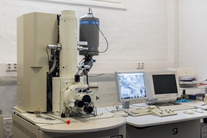
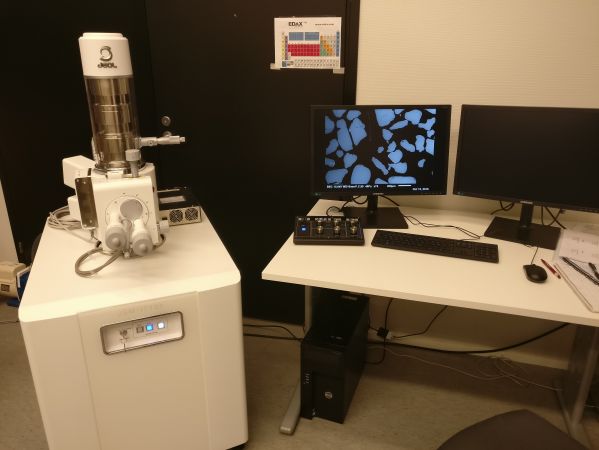
Scanning electron microscope SEM-EDS / WDS
Scanning Electron Microscope (SEM) and X-ray Analyzer (EDS / WDS) form a versatile analytical tool that allows for material surface analysis to be carried out very accurately. High resolution allows accurate image quality at very high magnifications, and an X-ray analyzer can simultaneously analyze elemental composition even up to a micrometre resolution.
Top Analytical has three electron microscopes, two of which are equipped with an EDS analyzer and a third device with four WDS analyzers (EPMA). They are also equipped with the basic SE and BSE -detectors.
SE-imaging
With Secondary Electrons (SE) a high resolution image can be produced and real time surface imaging is possible. The advantages of SE-imaging are very high resolution (up to 5 nm depending on the SEM and sample) and observation on topographical details with good 3-dimensional depth. Secondary electron are produced when sample material is bombarded with an electron beam which excites atoms that release their energy by emitting the secondary electrons.
- High resolution SEM-imaging
- Topographic details
- Magnification 20x – 200 000x
- Resolution 5 nm
BSE-imaging
With BackScattered Electrons (BSE) a real time imaging is also possible. The BS electrons are directly scattered from the atomic nucleus which swing the electrons back to a detector. The possibility of this is higher when the atom is heavier which means that the signal output will be low for light atoms (such as carbon) and high for heavy elements (like Pb). This is used to create a bse-image where difference in the elements in different phases can be observed as a contrast difference (dark/bright). BSE does not have as good resolution and lacks the 3 dimensional depth resolution in comparison to SE imaging
- Observing different phases
- Identifying and analysing particles / impurities
- Detecting heavy metals
EDS-analyzer
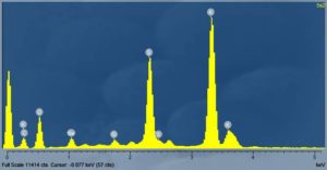
X-rays are always emitted in electron microscopy and it can be used to get information about the elemental composition of the sample simultaniuosly during imaging. EDS-analyzer (Energy Dispersive Spectrometer) counts all the incoming x-rays from a analysis point or area into a large energy scale spectrum which means all elements are calculated simultaniously (excluding H, He and Li). From this spectra the software can calculate elemental composition acurately. The sensitivity of EDS analyzer is approximately 0,1 – 0,5 p-% and spatial resolution about 1 micrometer.
- Point analysis
- Area analysis
- Elemental mapping
- Fast full scale spectra
WDS-analyzer
SEM-WDS system in Top Analytica is also called Electron Probe MicroAnalyzer (EPMA). WDS comes from Wavelength Dispersive Spectrometer which mean that this spectrometer analyzes only small section of the energy scale at a time. However the resolution from this area is much better than with EDS and therefore the sensitivity is much better (about 10 – 100 ppm). Typically there are multiple WDS-analyzers in one system (our EPMA has 5 WDS + 1 EDS) to gather multiple elemental data at a time.
- Low concentration elemental analysis
- Elemental mapping
- Point and area analysis
CI, Fe and O
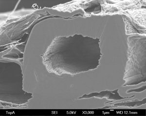
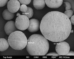
Particle profiling
SEM is the perfect tool to identify and profile particle feature such as dimensions, shapes and elemental composition. It is easy to determine lengths and angles with the software tools. Research in the small things can be key to product optimization.
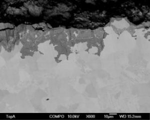
Corrosion samples
Corrosion is one of the biggest challenges faced in steel industry. To figuring out and overcoming the causes of corrosion SEM analysis is a great tool to begin. In this image a cross section of corroded steel is shown. An elemental mapping was done and it can be clearly seen that chlorine is right under the iron oxide area and it is the most likely corrosion accelerator in this case.
Elemental map: Chlorine, Iron and Oxygen
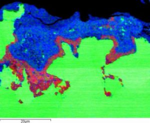
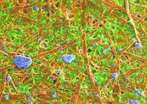
Elemental map of a paper surface
SEM image from the surface of a paper where CaCO3 (blue), caoline (green) and C + O (red) are seen.
Read the full case study here:
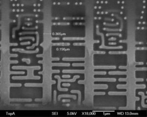
Cross section of a old processor
Nanoscale features can be seen in this cross section of an old processor component made with a Broad Ion Beam (BIB) system. Novel electronics go already down to 15 nm features that in addition to high resolution imaging system they also require super sensitive sample preparation.